硬脆材料複合加工技術
簡介 Introductions
碳化矽可應用在次世代功率元件中,為下世代功率半導體元件的關鍵材料。因高硬度及高耐化性等難加工特性,導致使生產率低,阻礙功率元件發展潮流。本技術建立複合式研拋製程平台,透過導入超音波輔助加工技術及大氣電漿輔助改質技術,可大幅提升碳化矽晶圓產能效率及有效降低製造成本。
Silicon carbide can be used in next-generation power components and is a key material for next-generation power components. Due to the difficult processing characteristics such as high hardness and high chemical resistance, the productivity is low and the development trend of power components is hindered. This technology establishes a hybrid-processing platform which includes of the ultrasonic assisted processing technology and atmospheric plasma assisted modification technology. It can greatly improve the production efficiency of silicon carbide wafers and effectively reduce manufacturing costs.
特色與創新 Characters and Innovations
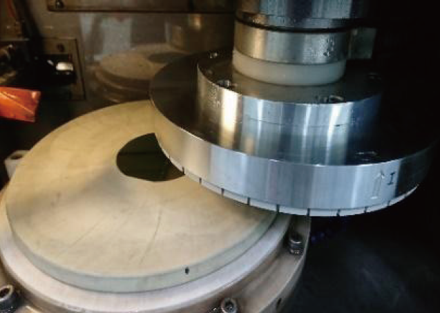
- 建立超音波輔助輪磨技術,可搭配高號數砂輪,達到高的材料移除率 > 10 μm /min,表面粗糙度 < 10nm。
- 透過大氣電漿改質拋光技術,電漿作用的面積 >200mm,拋光移除率 > 1.5μm/hr ,表面粗糙度 < 0.5nm。
- To establish the ultrasonic-assisted grinding technology, which can be matched with high-number grinding wheels and achieve high material removal rate > 10 μm/min, finished surface roughness < 10nm.
- Through atmospheric plasma modification polishing technology, the plasma action area is > 200mm, the polishing removal rate is > 1.5μm/hr, and the surface roughness is < 0.5nm.
應用與效益 Applications and Benefits
- 碳化矽晶圓、玻璃晶圓、鑽石基板。
- Silicon carbide wafers, Glass wafers, Diamond substrates.
聯絡 contact
更多資訊
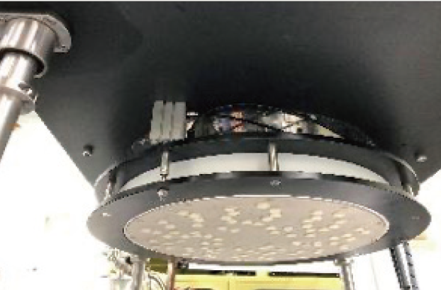
大氣電漿改質拋光組
Atmospheric plasma modified polishing module